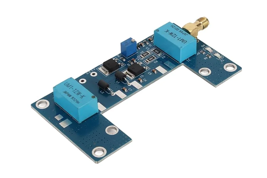
An RF PCB, or radio frequency printed circuit board, is a specialized type of PCB engineered to carry signals at high frequencies, typically in the range of megahertz (MHz) to gigahertz (GHz). These boards are essential in systems that require fast and precise signal transmission such as wireless communication, radar systems, satellite equipment, and RF amplifiers. Unlike standard PCBs, RF PCBs must be manufactured using specific materials and techniques to minimize signal loss and maintain signal integrity.
At high frequencies, even minor imperfections in the PCB layout, trace geometry, or material composition can lead to significant performance degradation. This is why RF PCBs must be designed with extreme accuracy, using materials like Rogers, Teflon, or other low-loss dielectric laminates that maintain a consistent impedance and reduce dielectric losses across the frequency range.
Key Design Considerations for RF PCBs
Designing an RF PCB involves more than just laying out traces and placing components. Engineers must carefully manage parameters such as impedance, crosstalk, signal integrity, and electromagnetic interference (EMI). Every element—from the trace width and spacing to the ground plane configuration—affects the performance of the circuit.
Signal paths in RF PCBs must be kept as short and direct as possible to avoid signal degradation. Controlled impedance is often necessary for transmission lines, requiring precise trace geometry and consistent dielectric material thickness. Proper shielding and grounding are also critical to isolate RF sections from noise or other circuit segments.
Additionally, passive components such as inductors and capacitors behave differently at RF frequencies, so their placement and values must be adjusted accordingly. RF simulation tools are often used in the design phase to predict how the board will perform before physical prototyping begins.
Common Materials Used in RF PCB Fabrication
The materials used in RF PCBs play a pivotal role in ensuring stable and accurate signal transmission. Traditional FR4 material is generally avoided in high-frequency designs due to its high dielectric loss and variability. Instead, manufacturers prefer advanced materials with stable dielectric constants, low dissipation factors, and minimal signal attenuation.
Some of the most common RF PCB materials include Rogers laminates, PTFE (Teflon), Arlon, and Taconic. Each of these materials offers unique properties, but all share the goal of supporting high-frequency operation with minimal signal loss. These materials are also chosen based on factors such as thermal performance, dimensional stability, moisture absorption, and cost.
In multilayer RF PCBs, different layers may use different materials to balance performance with manufacturability and cost. For instance, a hybrid stack-up may involve a combination of FR4 and Rogers to achieve an optimal balance between RF performance and mechanical strength.
Applications That Rely on RF PCBs
RF PCBs are integral to a wide range of industries that depend on high-speed signal transmission and wireless communication. In telecommunications, RF PCBs are used in mobile base stations, signal repeaters, and wireless routers. They also form the core of GPS systems, satellite communication modules, and radar systems used in both civilian and military applications.
In the medical field, RF PCBs enable technologies such as MRI machines, remote monitoring devices, and wireless implants. Automotive electronics, particularly in connected vehicles and advanced driver-assistance systems (ADAS), also leverage RF PCBs to facilitate real-time communication and radar-based sensing.
Consumer electronics such as smartphones, Bluetooth devices, smartwatches, and Wi-Fi-enabled gadgets are among the most common uses of RF PCBs today. As the demand for faster and more reliable wireless communication increases, so too does the importance of precision-engineered RF boards.
Challenges in RF PCB Manufacturing
Manufacturing an RF PCB is a delicate process that demands precision, cleanliness, and expertise. Every step—etching, drilling, plating, lamination, and soldering—must be controlled to avoid introducing defects that could affect signal transmission. For instance, rough copper surfaces or misaligned layers can disrupt impedance and introduce signal reflection.
RF PCBs also require tighter tolerances for trace widths, dielectric thickness, and conductor spacing. This means manufacturers must use advanced equipment and process controls to ensure consistency. Additionally, material handling becomes more critical, as RF laminates tend to be softer and more prone to dimensional changes than standard materials.
Testing RF PCBs is also more complicated than testing standard boards. Vector network analyzers (VNAs) and other high-frequency test equipment are needed to evaluate signal behavior, phase stability, and return loss. Only highly experienced fabrication partners can consistently deliver the quality expected in high-frequency applications.
Choosing the Right RF PCB Manufacturer
Finding the right rf pcb manufacturer is critical for achieving peak performance in your high-frequency projects. Not all PCB manufacturers have the expertise, materials, or equipment required to handle the unique challenges of RF PCB production. Whether you’re building prototypes or scaling for mass production, working with a trusted RF PCB manufacturer ensures your designs will be manufactured to exacting standards with the precision necessary for high-frequency performance. Be sure to partner with a provider who understands both the technical and application-specific demands of RF PCBs to get the best results for your product.


